- 您现在的位置:买卖IC网 > Sheet目录3879 > DSPIC30F6013T-20I/PF (Microchip Technology)IC DSPIC MCU/DSP 132K 80TQFP
2006 Microchip Technology Inc.
DS70117F-page 139
dsPIC30F6011/6012/6013/6014
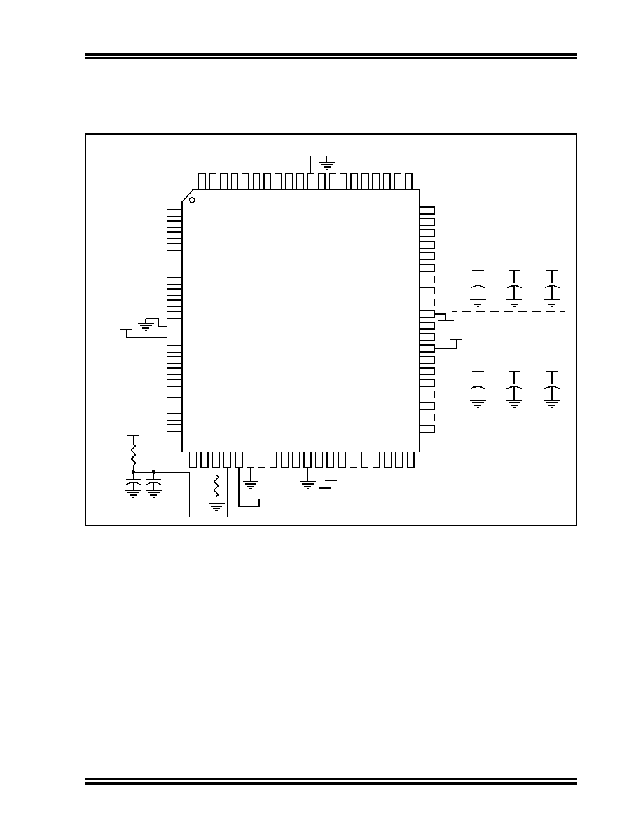
The following figure depicts the recommended circuit
for the conversion rates above 200 ksps. The
dsPIC30F6014 is shown as an example.
FIGURE 19-2:
ADC VOLTAGE REFERENCE SCHEMATIC
The configuration procedures below give the required
setup values for the conversion speeds above 100
ksps.
19.7.1
200 KSPS CONFIGURATION
GUIDELINE
The following configuration items are required to
achieve a 200 ksps conversion rate.
Comply with conditions provided in Table 19-2.
Connect external VREF+ and VREF- pins following
the recommended circuit shown in Figure 19-2.
Set SSRC<2.0> = 111 in the ADCON1 register to
enable the auto convert option.
Enable automatic sampling by setting the ASAM
control bit in the ADCON1 register.
Write the SMPI<3.0> control bits in the ADCON2
register for the desired number of conversions
between interrupts.
Configure the ADC clock period to be:
by writing to the ADCS<5:0> control bits in the
ADCON3 register.
Configure the sampling time to be 1 TAD by
writing: SAMC<4:0> = 00001.
The following figure shows the timing diagram of the
ADC running at 200 ksps. The TAD selection in conjunc-
tion with the guidelines described above allows a con-
version speed of 200 ksps. See Example 19-1 for code
example.
72
74
73
V
DD
V
SS
69
68
67
66
65
64
63
62
61
20
2
3
4
5
6
7
8
9
10
VSS
VDD
13
14
15
16
50
49
VDD
47
46
45
44
21
41
40
39
38
37
36
35
34
V
RE
F
-
V
RE
F
+
AV
DD
AV
SS
27
28
29
30
V
SS
V
DD
33
17
18
19
75
1
57
56
55
54
53
52
VSS
60
59
58
43
42
76
78
77
79
22
80
dsPIC30F6014
VDD
R2
10
C2
0.1
μF
C1
0.01
μF
R1
10
C8
1
μF
VDD
C7
0.1
μF
VDD
C6
0.01
μF
AVDD
C5
1
μF
AVDD
C4
0.1
μF
AVDD
C3
0.01
μF
See Note 1:
Note 1: Ensure adequate bypass capacitors are provided on each VDD pin.
1
(14 + 1) x 200,000
= 334 ns
发布紧急采购,3分钟左右您将得到回复。
相关PDF资料
DSPIC30F6012T-30I/PF
IC DSPIC MCU/DSP 144K 64TQFP
DSPIC30F6012T-20I/PF
IC DSPIC MCU/DSP 144K 64TQFP
DSPIC30F6011T-30I/PF
IC DSPIC MCU/DSP 132K 64TQFP
DSPIC30F6011T-20I/PF
IC DSPIC MCU/DSP 132K 64TQFP
DSPIC30F6010T-30I/PF
IC DSPIC MCU/DSP 144K 80TQFP
DSPIC30F6010T-20I/PF
IC PSPIC MCU/DSP 144K 80TQFP
PIC16C56A-20/P
IC MCU OTP 1KX12 18DIP
PIC16C621A-04I/P
IC MCU OTP 1KX14 COMP 18DIP
相关代理商/技术参数
DSPIC30F6013T-30I/PF
功能描述:数字信号处理器和控制器 - DSP, DSC 30MHz 132KB Flash RoHS:否 制造商:Microchip Technology 核心:dsPIC 数据总线宽度:16 bit 程序存储器大小:16 KB 数据 RAM 大小:2 KB 最大时钟频率:40 MHz 可编程输入/输出端数量:35 定时器数量:3 设备每秒兆指令数:50 MIPs 工作电源电压:3.3 V 最大工作温度:+ 85 C 封装 / 箱体:TQFP-44 安装风格:SMD/SMT
DSPIC30F6014-20E/PF
功能描述:数字信号处理器和控制器 - DSP, DSC 30MHz 132KB Flash RoHS:否 制造商:Microchip Technology 核心:dsPIC 数据总线宽度:16 bit 程序存储器大小:16 KB 数据 RAM 大小:2 KB 最大时钟频率:40 MHz 可编程输入/输出端数量:35 定时器数量:3 设备每秒兆指令数:50 MIPs 工作电源电压:3.3 V 最大工作温度:+ 85 C 封装 / 箱体:TQFP-44 安装风格:SMD/SMT
DSPIC30F6014-20I/P
制造商:Microchip Technology Inc 功能描述:MCU - Rail/Tube
DSPIC30F6014-20I/PF
功能描述:数字信号处理器和控制器 - DSP, DSC 20MHz 144KB Flash RoHS:否 制造商:Microchip Technology 核心:dsPIC 数据总线宽度:16 bit 程序存储器大小:16 KB 数据 RAM 大小:2 KB 最大时钟频率:40 MHz 可编程输入/输出端数量:35 定时器数量:3 设备每秒兆指令数:50 MIPs 工作电源电压:3.3 V 最大工作温度:+ 85 C 封装 / 箱体:TQFP-44 安装风格:SMD/SMT
DSPIC30F6014-20I/PF
制造商:Microchip Technology Inc 功能描述:16BIT 20MIPS DSPIC SMD 30F6014
DSPIC30F6014-30I/PF
功能描述:数字信号处理器和控制器 - DSP, DSC 30MHz 144KB Flash RoHS:否 制造商:Microchip Technology 核心:dsPIC 数据总线宽度:16 bit 程序存储器大小:16 KB 数据 RAM 大小:2 KB 最大时钟频率:40 MHz 可编程输入/输出端数量:35 定时器数量:3 设备每秒兆指令数:50 MIPs 工作电源电压:3.3 V 最大工作温度:+ 85 C 封装 / 箱体:TQFP-44 安装风格:SMD/SMT
DSPIC30F6014-30I/PF
制造商:Microchip Technology Inc 功能描述:16BIT 30MIPS DSPIC SMD 30F6014
dsPIC30F6014A-20E/PF
功能描述:数字信号处理器和控制器 - DSP, DSC 20MIPS 144 KB RoHS:否 制造商:Microchip Technology 核心:dsPIC 数据总线宽度:16 bit 程序存储器大小:16 KB 数据 RAM 大小:2 KB 最大时钟频率:40 MHz 可编程输入/输出端数量:35 定时器数量:3 设备每秒兆指令数:50 MIPs 工作电源电压:3.3 V 最大工作温度:+ 85 C 封装 / 箱体:TQFP-44 安装风格:SMD/SMT